Research Facilities
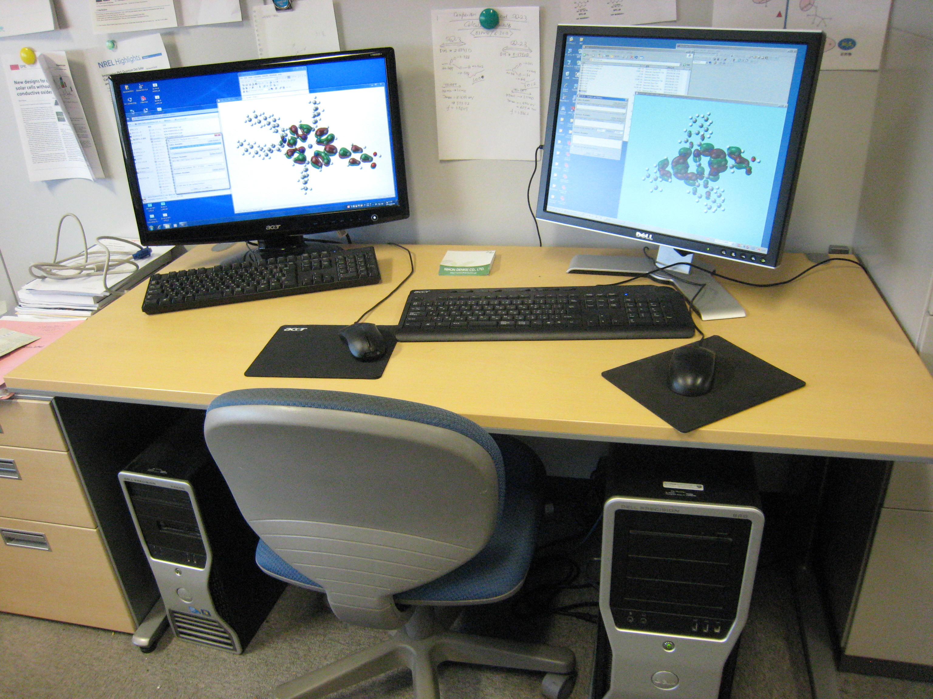
Quantum Chemical Caluclations
Chem Office; Gaussian Ver 16.
Design of Photofunctional and Organic Semiconducting Materials for their Potential Applications towards Next-generation Solar Cells, Organic Electronic Devices and Sensing;Molecular Orbital calculation (HOMO, LUMO and Energy Band gap; Structural Optimization; Simulation of FTIR, NMR, Circular Dichroism and Electronic Absorption spectra.
Synthesis of Functional Materials
Fume Hoods
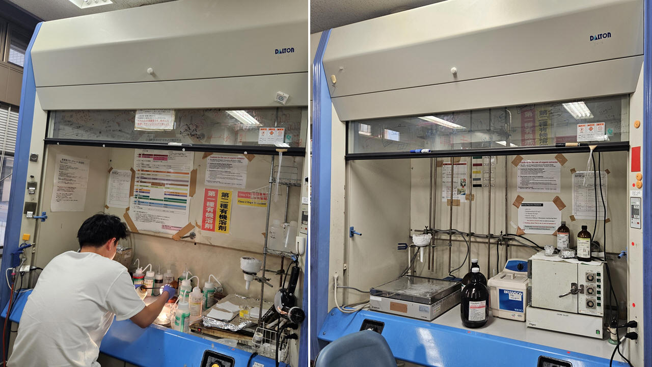
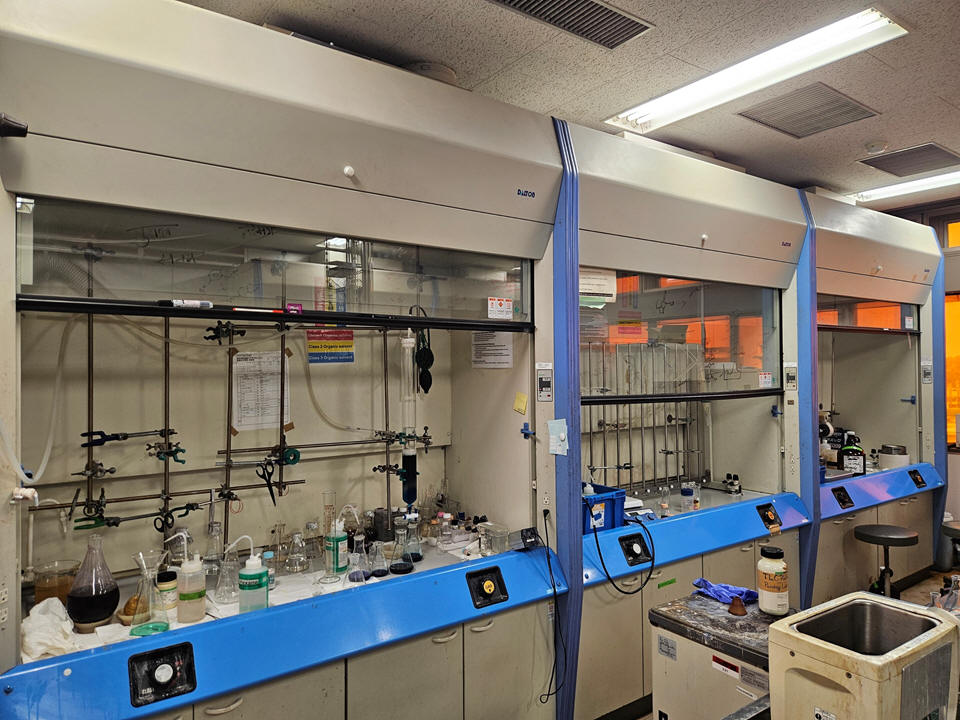
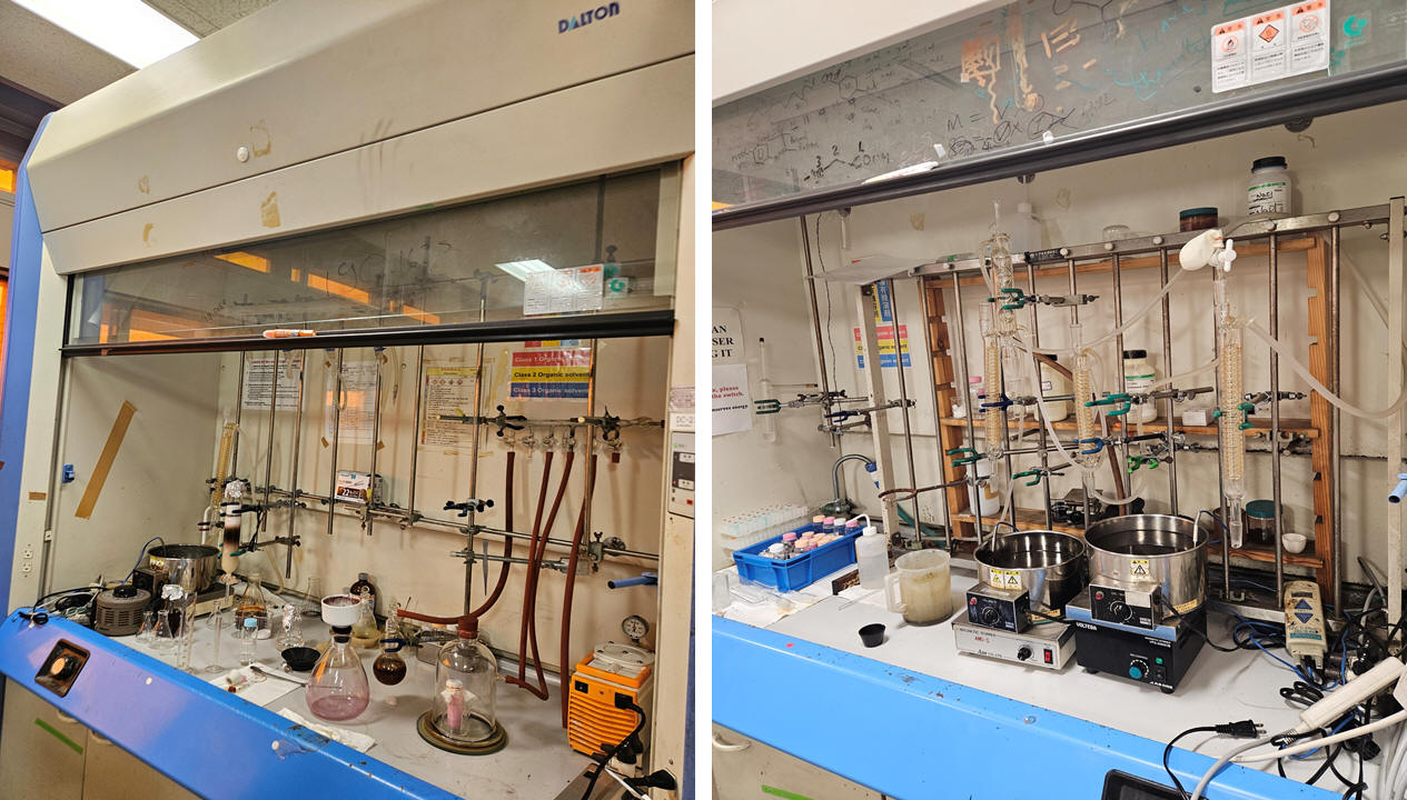
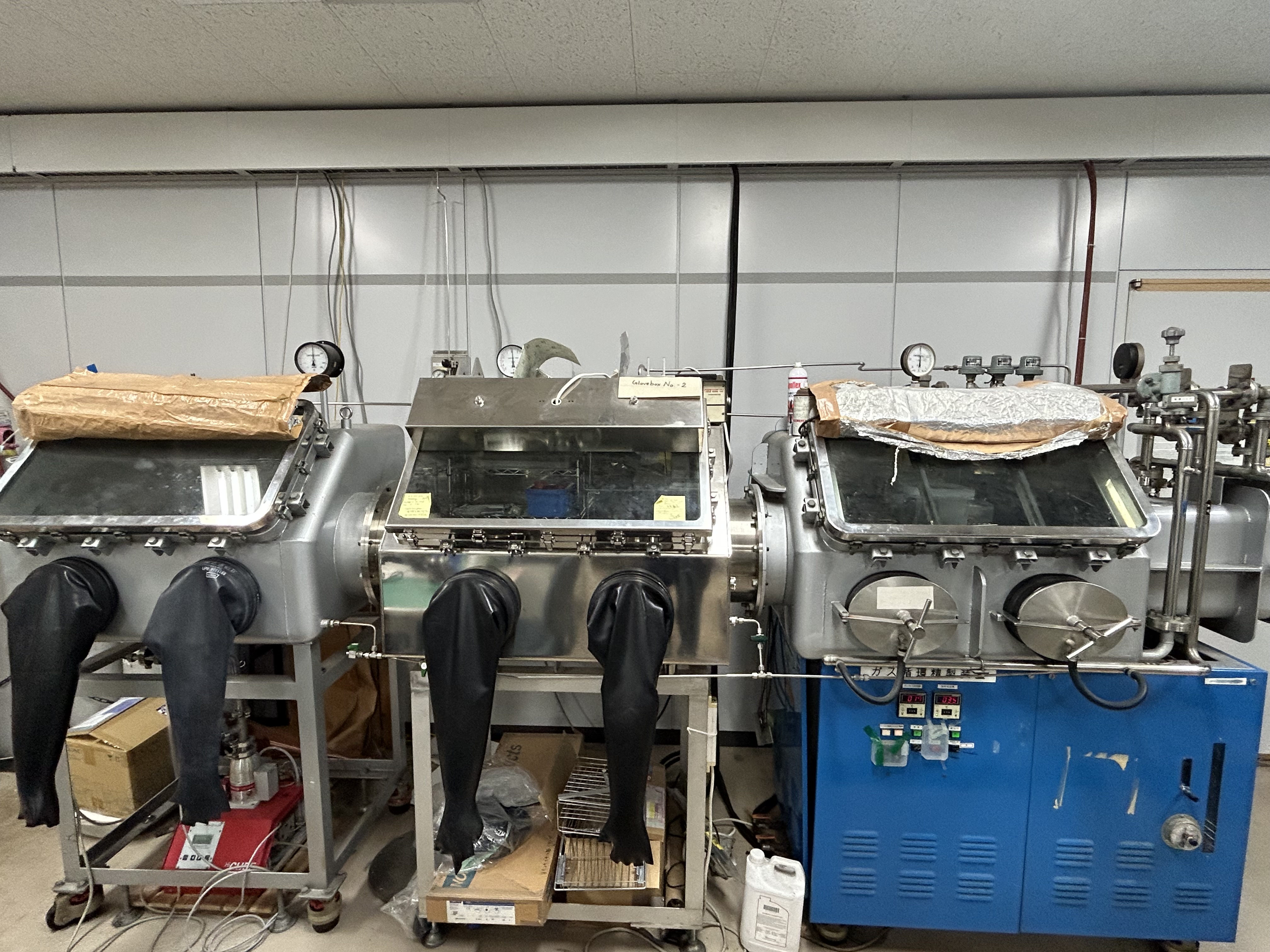
Thin Film Fabrication; Inorganic and organic Synthesis, Possibility of reaction under vacuum and inert atmosphere, Synthesis of organic and photofunctional materials and polymers.
Material Characterizations
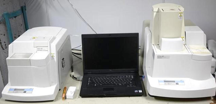
High Performance Liquid Chromatography [HPLC]
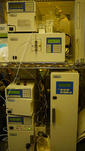
Analytical HPLC equipped with UV and Photodiode Array detectors; Characterization of intermediates, impurities and final products. Determination of purity of final products. Utilization of PDA detector allows the real monitoring of impurities and products by simultaneous measurement of electronic absorption spectra.
Electronic Absorption Spectroscopy [V-570, V550, JASCO]
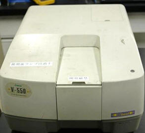
Instrument used for measurement absorption spectra in UV-visible and infrared wavelength region. Possible to use both of solid and liquid samples. Possibility of measuing polarized absorption spectra utilizing Glan-Thomson Prism. Used for the characterization of materials based on there characteristic electronic transitions qualitatively as well as quantitatively.
Differential Scanning Calorimetry (DSC-7, Perkin Elmer) and Thermo-Gravimetric Analysis (TG-DTA)
Instruments associated with the investigation of thermal properties of materials. Currently being used for the measurement thermal stability, melting and degradation temperature and phase changes during thermal cycles.
Electrochemical Measurements
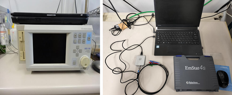
This instrument is used for various electroanalysticsl analysis such Cyclic-Voltametry, Linear Sweep Voltammetry, Pulse Voltammetry and Electrochemical Impedance Measurements..
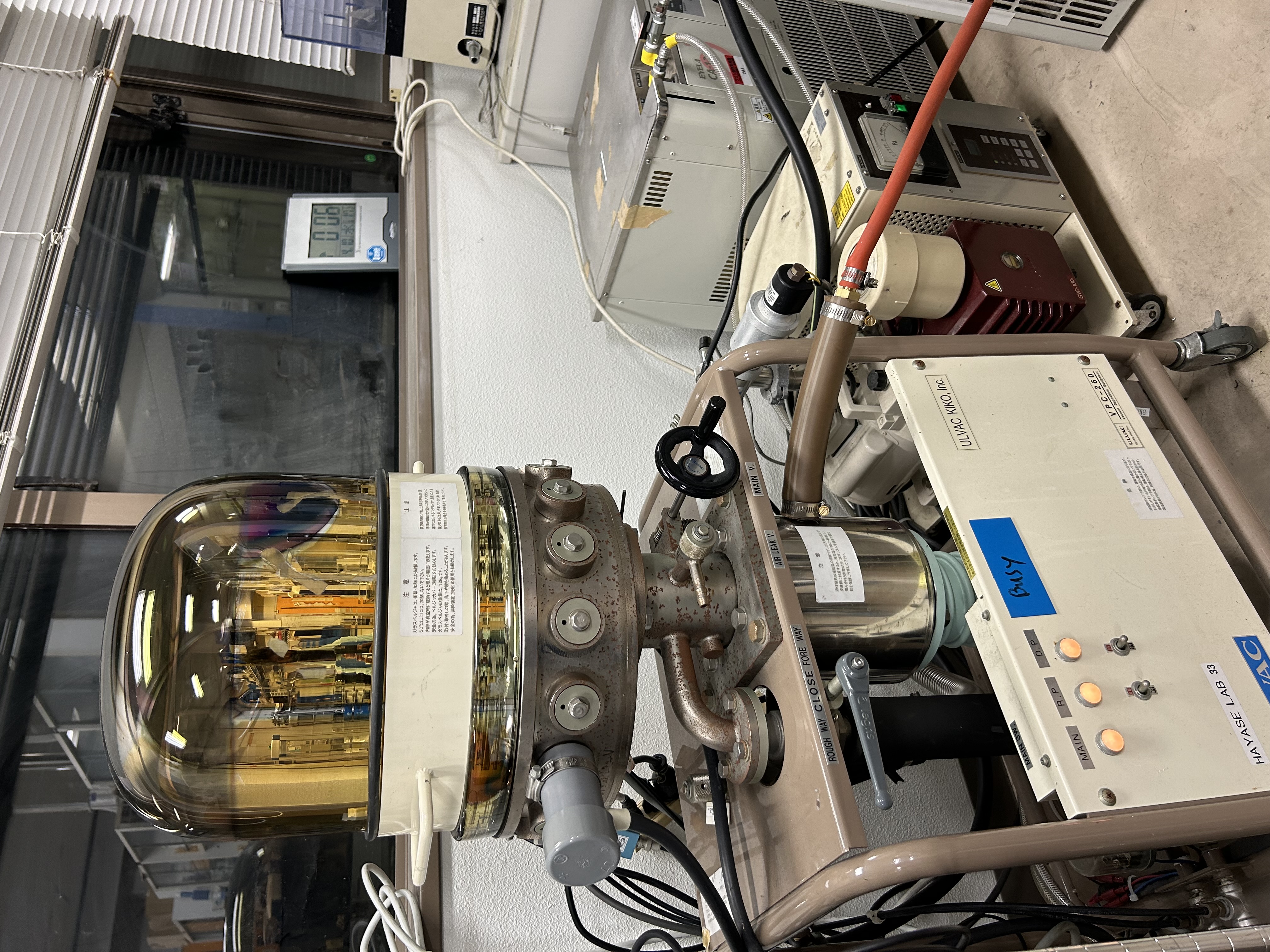
Organic Electronic Device Fabrication and Characterization
Spin-Coater and Nano-Dip Coater
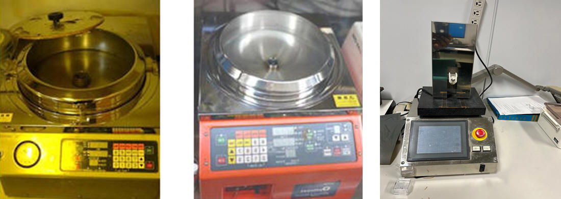
Thin film fabrication using solution-processable photo-fucntional organic materials along with polymeric materials. Using Nano-dip coater we can prepare homogenious and large area thin films with propmoted molecular self-assembly by controlling concentration, temperature and lifting speed.
Friction Transfer
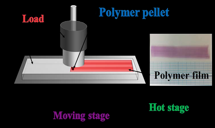
This is and an envronment-friendly and solvent-less technique for the fabrication of oriented and large area thin films. Very suitable for functional materials which are insoluble in organic solvents.Due to use of sheer forces, the fabricated thin films are generally face-on oriented.
Floating Film Transfer
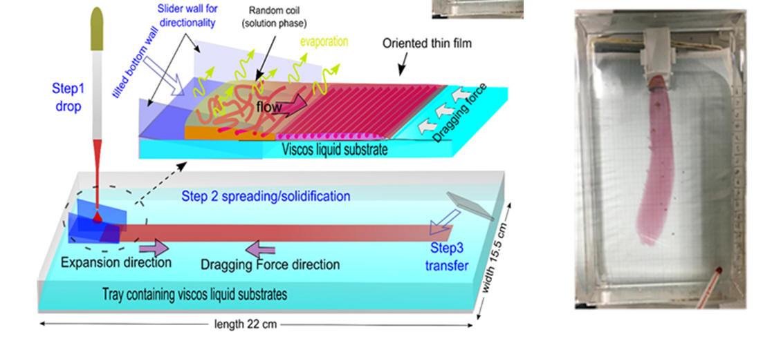
This is very interesting and cost-effective solution-based technique for the facile fabrication of the large area, homogenious oriented thin films. This does not require any specific instrument and extent of the orientation can be easily tuned by controlling the viscosity of material and liquid subphase, temperature and concentration of the target materials.
2D-Positional Mapping System
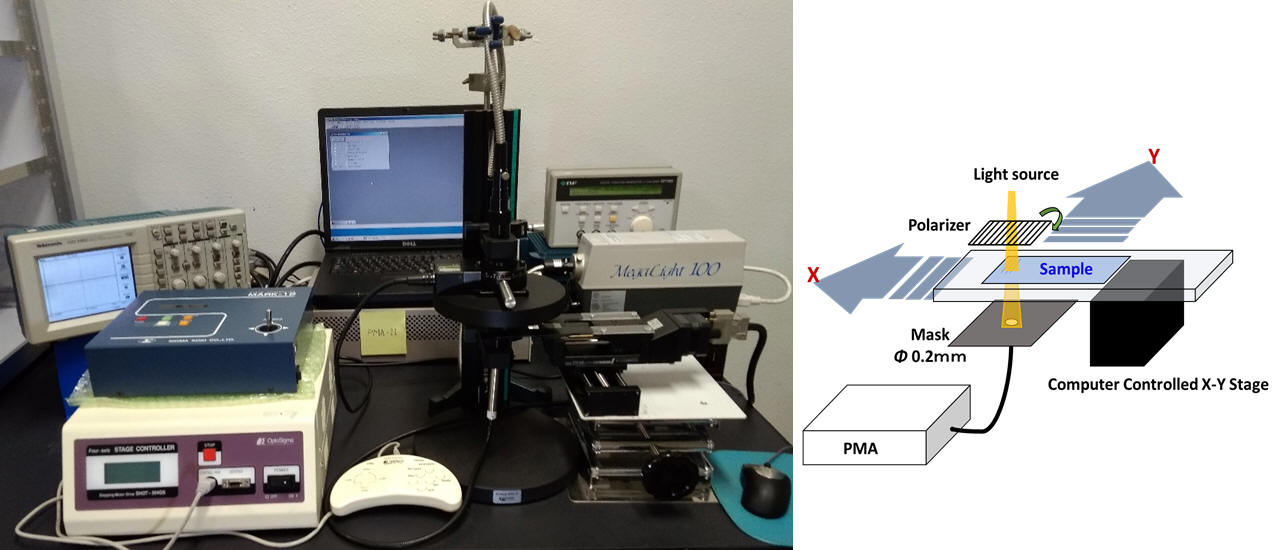
This is an in-house developed system for the swift and facile mapping of the thin-film uniformity and distribution of the molecular orientation in the large area thin films. Effectiveness of this system has been validated by using standard electronic absorption measuremnt system and its versatility has been tested uisng oriented and non-oriented thin films prepared by various methods such as spin-coating, dip-coating, friction transfer and floating film transfer methods.
Fabrication & Characterization of Organic Electronic Devices
This system is being used for device fabrication under inert atmosphere having controlled oxygen and moisture. The system is equipped, balance, hot-plate and spin-coater with automatic Ar flushing to maintain the 24X7 round the clock inert atmosphere for device fabrication.
Physical Vapour deposition
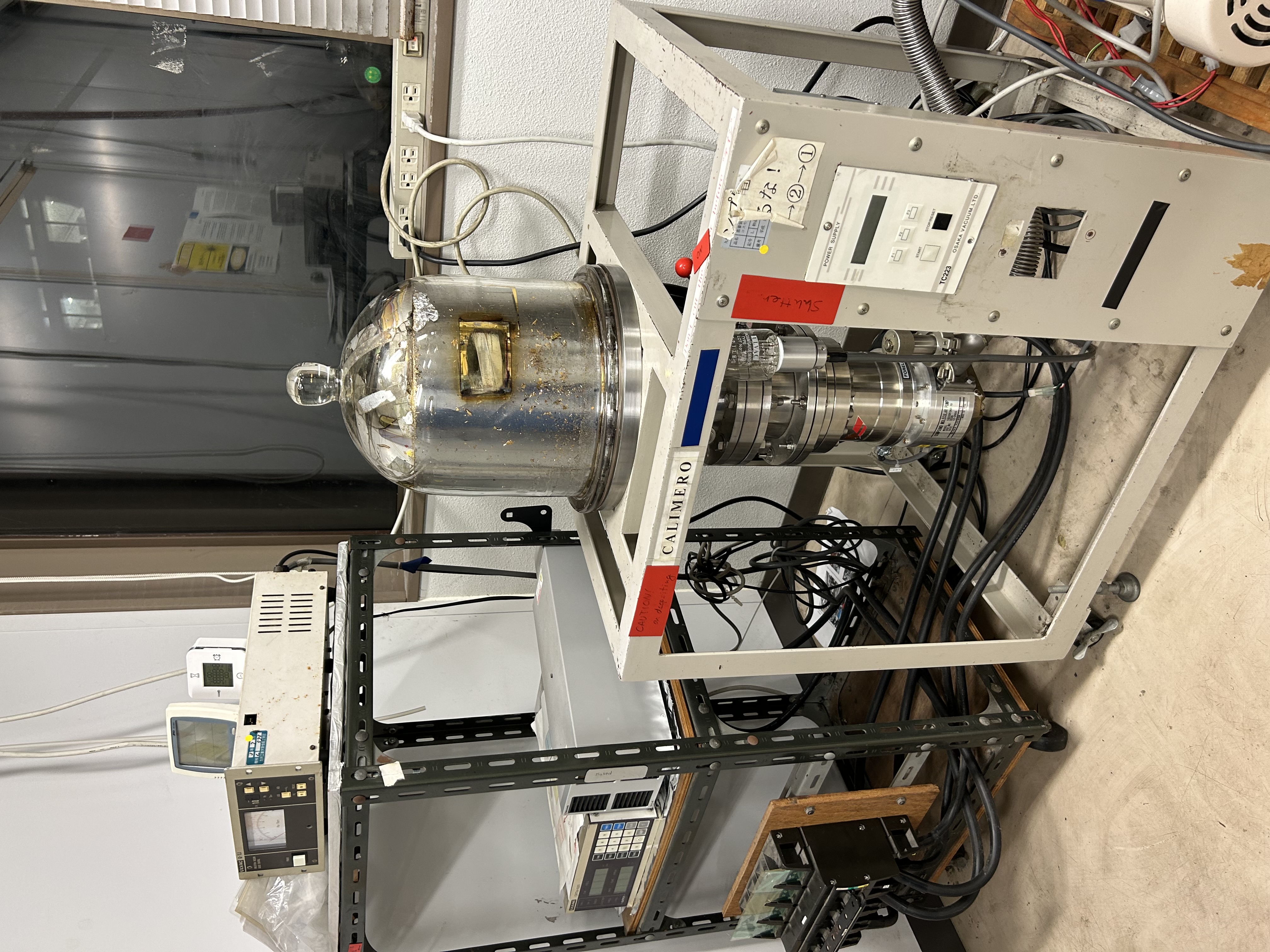
This system is used for the deposition of thin films of desired metals and organic materials to complete the organic electronic devices.
UV-Ozone Surface Cleaner & Ultrsonic Shouldering Machine
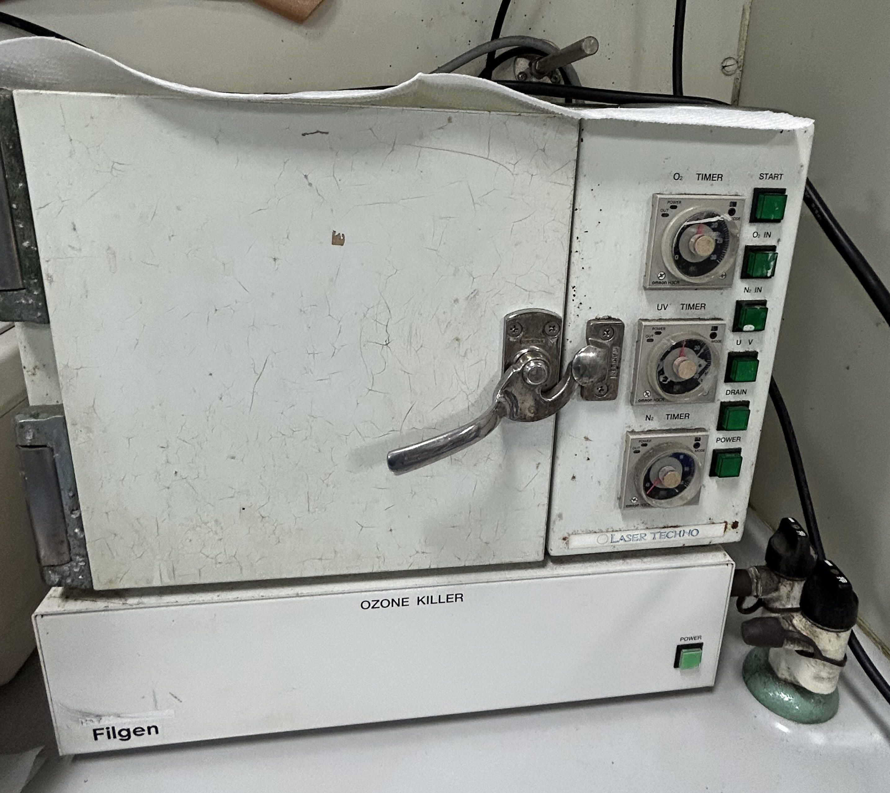
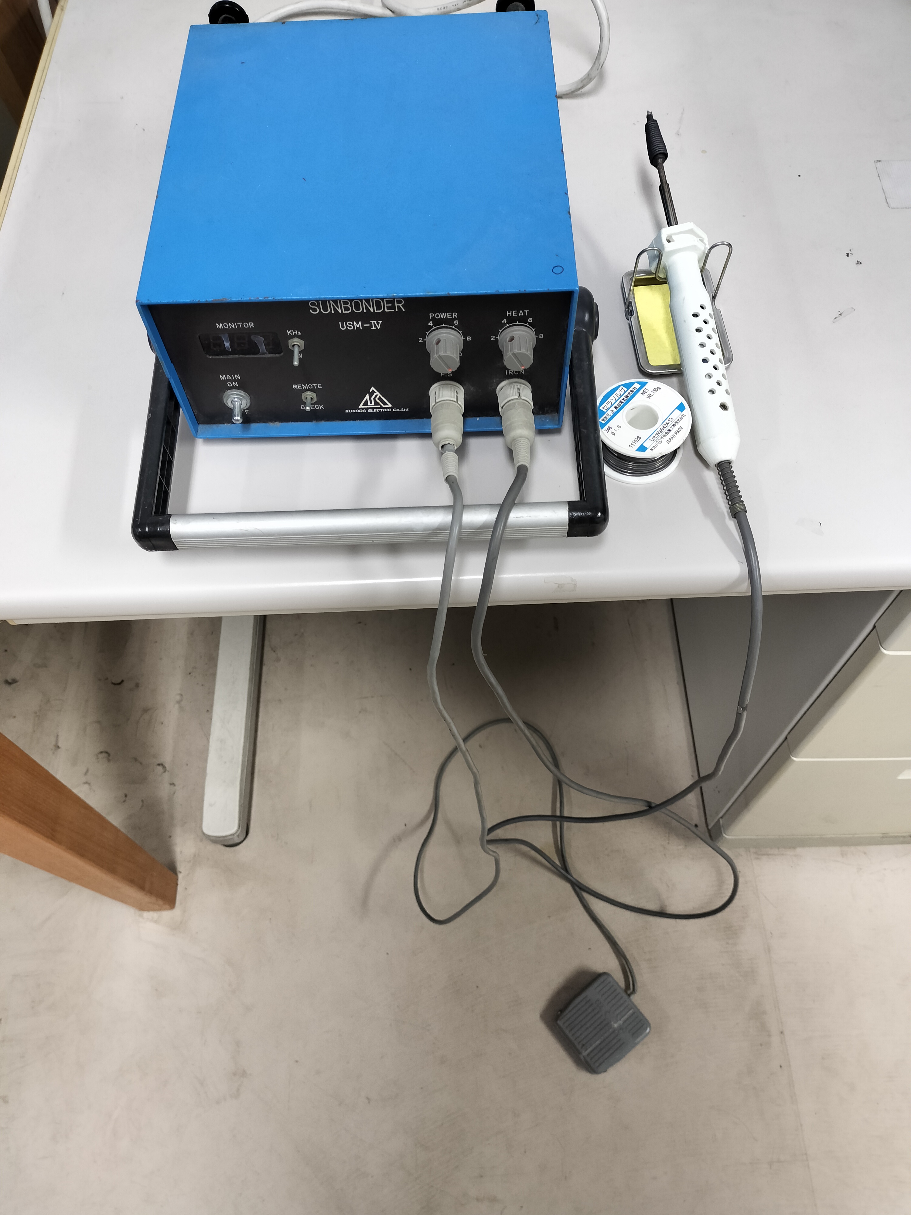
Left UV-Ozone cleaner for removing surface impurities and making the surface hydrophilic. On the other hand, righ is ultrasonic shouldering machine for effective shouildering of contact wires of the device elements.
Electrical Characterization
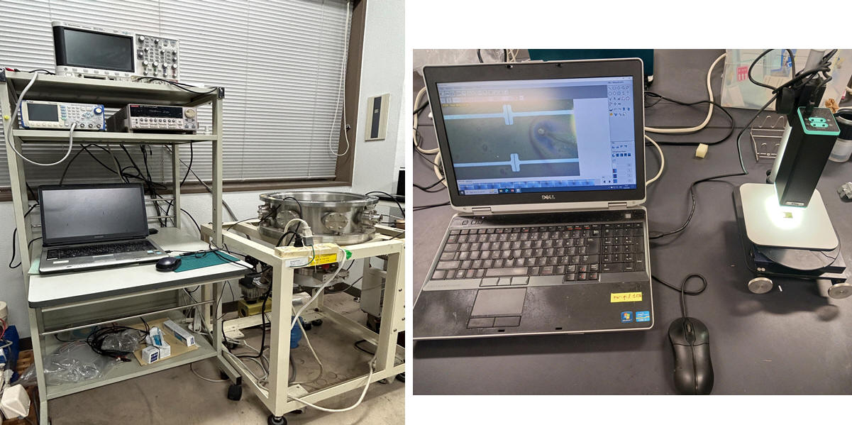
Left: Electrical characterization organic electronic devices such as resistors, capacitors, diodes and transitors in vacuum using in-house developed and customizable measurement programs. Right: Computer controlled digital microscope with maximum 390X magnification and autofocus control.
Opto-electrical Characterization
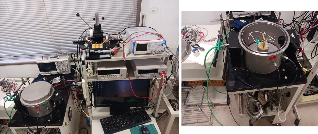
Combined optical and electrical characterization organic electronic devices uisng continuous and pulsed light of tunable wavelength from ultravoilet and near infrared under vacuum..
Solar Cell Fabrication & Characterization
Screen Printing and Thickness Profiling
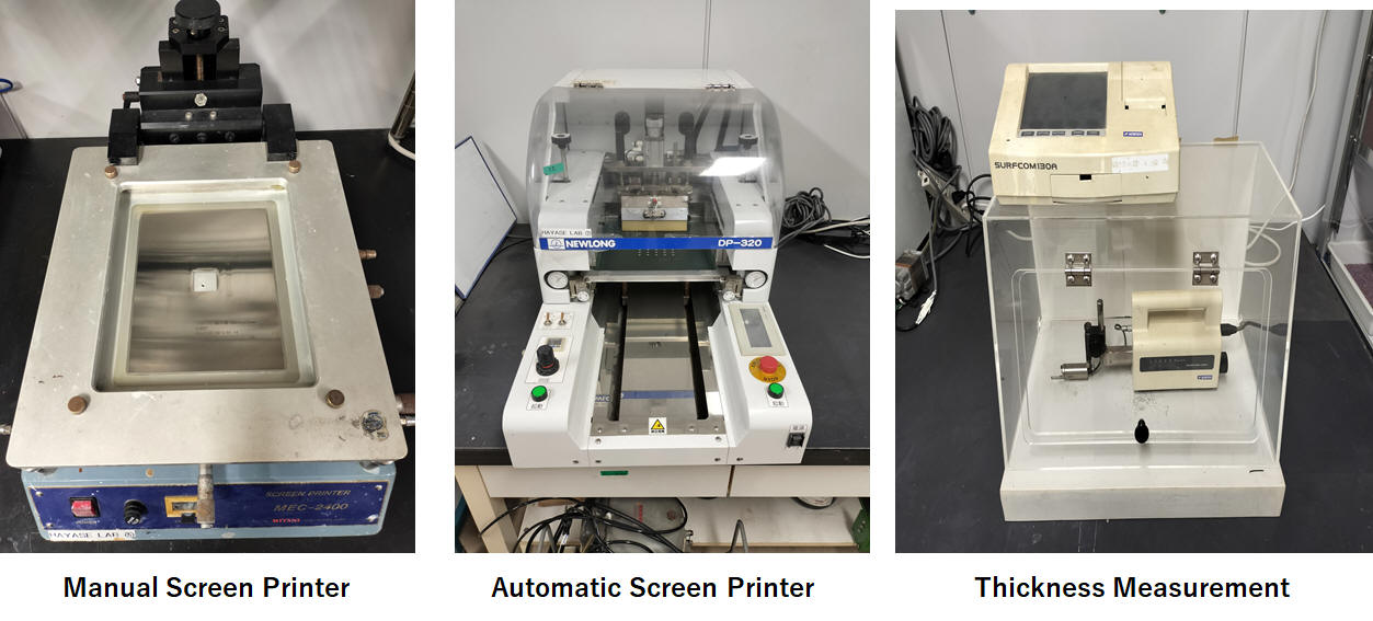
Screen printer is used for the fabrication of thin films of mesoporous wide band gap semicondcutors like TiO2, ZnO and SnO2 etc in manual (left) and auto(middle) modes. Finally, thickness of the of the prepared thin films is measured using surface profiler (right).
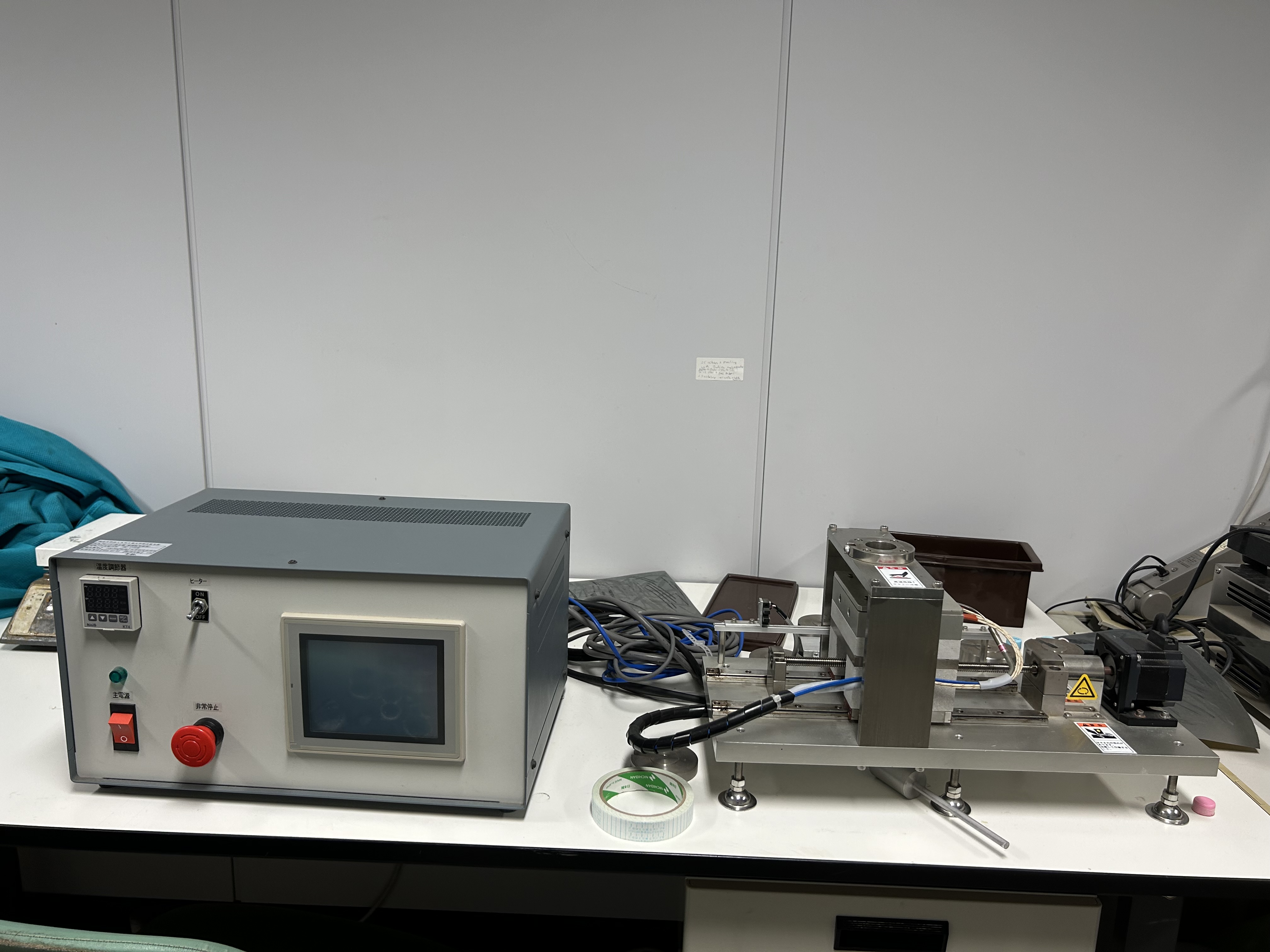
Drilling, Sintering & Sealing
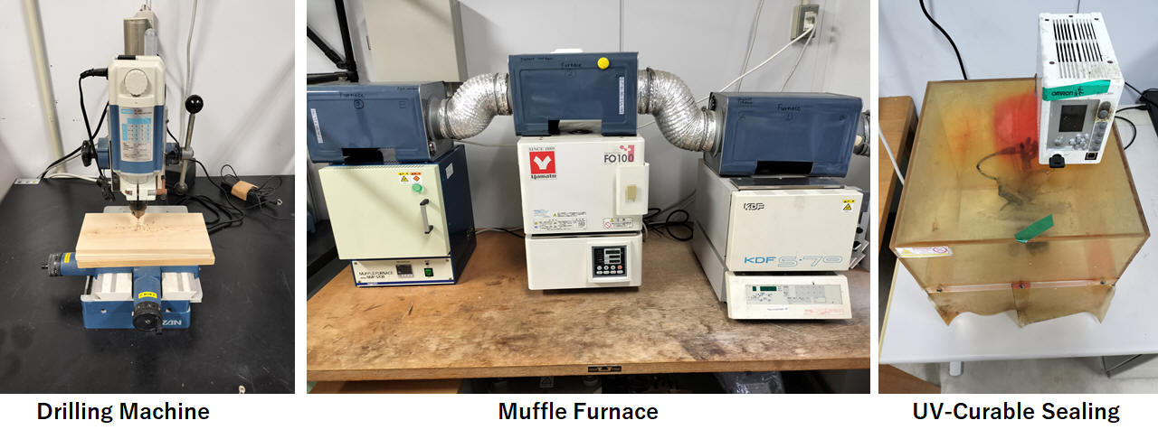
Drilling machine to make holes in metal or glass (left), programmable mufle furnace for sintering the films with upper temeperature up to 1200 degree celsius (middle) and sealing the devices uisng UV-curable resin (right).
Integrated Solar Simulator (JIS C 8912 Class A)
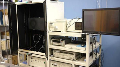
This is single point solution for photovoltaic characterization of solar cells equipped with measurement for both of the I-V characteristics and Incident photon to current conversion efficiency (IPCE) also known as Photo-action spectrum. It is capable of measuring the IPCE from 300-1100 nm.
Portable Solar Simulators (1 Sun & Indoor Light)
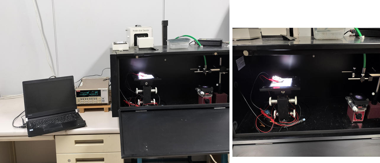
Portable and Table-top I-V measutemenst system uisng simulated one Sun (left) and low-intensity fluorescent light sources (right) for outdore and indoor photovolatic measurements.